Buku Persamaan Ic Dan Transistor Amplifier Circuits
Beautiful Gallery Of Buku Persamaan Ic Dan Transistor – From the thousand Shots on the internet regarding buku persamaan ic dan transistor, we all offer the most valuable libraries having best possible resolution simply for our readers, and now this images,in fact, regarded as one of stocks selections inside our good-looking photos gallery in relation to Beautiful Gallery Of Buku Persamaan Ic Dan Transistor. I feel you might love it. Beautiful Pic (Buku Persamaan Ic Dan Transistor Fresh Read N Write Membuat Power Suplay 5 Volt) formerly is generally labelled along with: written simply by Raymond Gibson at 2017-12-04 05:33:18. To get lots of models inside Beautiful Gallery Of Buku Persamaan Ic Dan Transistor shots gallery make sure you comply with that website hyperlink. If you like this post, then please share with your friends.
Contents • • • • • Overview [ ] ' as the term is currently used refers to a monolithic IC which differs notably from a HIC in that a HIC is fabricated by inter-connecting a number of components on a substrate whereas an IC's (monolithic) components are fabricated in a series of steps entirely on a single wafer which is then diced into chips. Some hybrid circuits may contain monolithic ICs, particularly (MCM) hybrid circuits. Hybrid circuits are often encapsulated in, as shown in the photo. A hybrid circuit serves as a component on a PCB in the same way as a monolithic; the difference between the two types of devices is in how they are constructed and manufactured. The advantage of hybrid circuits is that components which cannot be included in a monolithic IC can be used, e.g., capacitors of large value, wound components, crystals, inductors. Is often used as the interconnecting medium for hybrid integrated circuits. The use of screen printed thick film interconnect provides advantages of versatility over thin film although feature sizes may be larger and deposited resistors wider in tolerance.
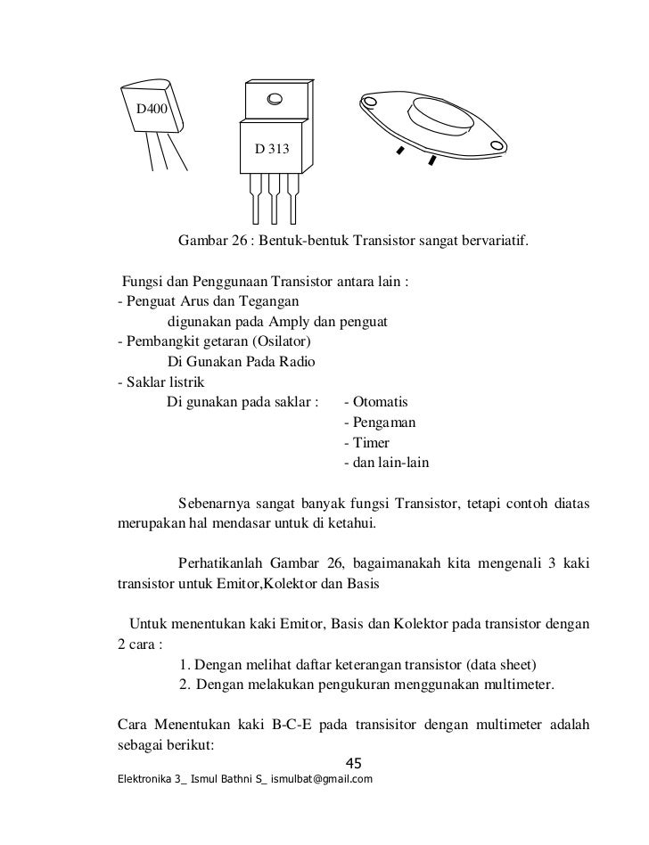
Simple audio amplifier circuit diagram using transistor. Buku persamaan ic dan transistor amplifier with symbol staffengineer. (integrated circuits), tdv (transistor, FET). Mengenalnya masih berupa “Buku Persamaan Semikonduktor ( IC, transistor. Komponen ini mempunyi banyak fungsi di dunia elektronik, seperti amplifier, switching (saklar), sinyal modulasi, stabilitas tegangan, dll.
Multi-layer thick film is a technique for further improvements in integration using a screen printed insulating dielectric to ensure connections between layers are made only where required. One key advantage for the circuit designer is complete freedom in the choice of resistor value in thick film technology. Planar resistors are also screen printed and included in the thick film interconnect design. The composition and dimensions of resistors can be selected to provide desired values.
Embed Facade on your website. Stencyl is the easiest way to create games for mobile, web and desktop without code. Learn More Download. Forums; Stencylpedia. Play Facade and become an actor in an interactive virtual drama! Can you help Trip and Grace save their marriage? Download free full version, read about the game, and view user reviews. Free facade game no download. Download free PC / computer Games: facade no DOWNLOAD List of Free PC Games for Download All Categories Action Games Adventure Games Arcade Games Board Games Cards Games Demo Games Educational Games First Person Shooter (FPS) Flight and Space Horror Games Kids Games Online Games Puzzle Games Racing Games Role Playing Game (RPG) Simulation Games.
The final resistor value is determined by design and can be adjusted. Once the hybrid circuit is fully populated with components, fine tuning prior to final test may be achieved by active laser trimming.
Thin film technology was also employed in the 1960s. Ultra Electronics manufactured circuits using a silica glass substrate. A film of tantalum was deposited by sputtering followed by a layer of gold by evaporation. The gold layer was first etched following application of a photo resist to form solder compatible connection pads. Resistive networks were formed, also by a photo resist and etching process.
Ultraman Cosmos Vs Ultraman Justice The Final Battle. Ultraman Cosmos vs. Ultraman Justice: The Final Battle Sub Indo 22.89 MB. Download Song Links or other sites. Ultraman Cosmos vs. Ultraman Justice: The Final Battle Sub Indo Nanas. [ENG SUB] Ultra Galaxy Legend. Ultraman Nexus VS Dark Mephisto Zwei - Duration. Download Ultraman Cosmos Sub Indo atau Bahasa Indonesia Batch Paket Google Drive HD Bluray BD 1080P 720P 480P 360P MKV MP4 3GP MisterKuhaku Download Power Rangers, Kamen Rider, Super Sentai, Ultraman, Metal Hero, Anime, Marvel, DC, Kartun, Tokusatsu Semua Lengkap Subtitle Bahasa Indonesia. Ultraman Cosmos The Final Battle Sub Indonesia. Ultraman Justice Crusher & Cosmos Future TAG Team Mode ★Play ウルトラマン FE3 - Duration. [ENG SUB] Ultra Galaxy Legend. Download ultraman cosmos vs ultraman justice sub indo full. Ultraman Cosmos vs. Ultraman Justice: The Final Battle Sub Indo. Download Ultraman Cosmos vs. Ultraman Justice: The Final Battle Sub Indo MP4. November 18, 2018.

These were trimmed to a high precision by selective adonization of the film. Capacitors and semiconductors were in the form of LID (Leadless Inverted Devices) soldered to the surface by selectively heating the substrate from the underside. Completed circuits were potted in a diallyl phthalate resin. Several customized passive networks were made using these techniques as were some amplifiers and other specialized circuits. It is believed that some passive networks were used in the engine control units manufactured by Ultra Electronics for Concorde.
Some modern hybrid circuit technologies, such as -substrate hybrids, allow for embedding of components within the layers of a multi-layer substrate in addition to components placed on the surface of the substrate. This technology produces a circuit that is, to some degree,. Steps in manufacturing Solid Logic Technology hybrid wafers used in the and other IBM computers of the mid-1960s. The process starts with a blank ceramic wafer 1/2 inch square. Circuits are laid down first, followed by resistive material. The circuits are metalized and the resistors trimmed to the desired value. Then discrete transistors and diodes are added and the package encapsulated.